

Introduction
In the paper Compute-in-Memory Computational Devices, we compared compute-in-memory with alternate architectures and showed that compute-in-memory (CIM) can offer significant advantages in power and performance for many applications. In this paper, we will review GSI's CIM Gemini® associative processing technology and show how it can be applied to a wide range of applications.
Compute-In-Memory (CIM) Review
GSI's CIM Gemini® associative processing technology is based on In-Memory Compute (IMC) and is implemented in the Gemini-I® and Gemini-II® devices. The technology is based on the Tanimoto distance measure and is designed for AI inference and other applications that require high throughput and low power consumption.
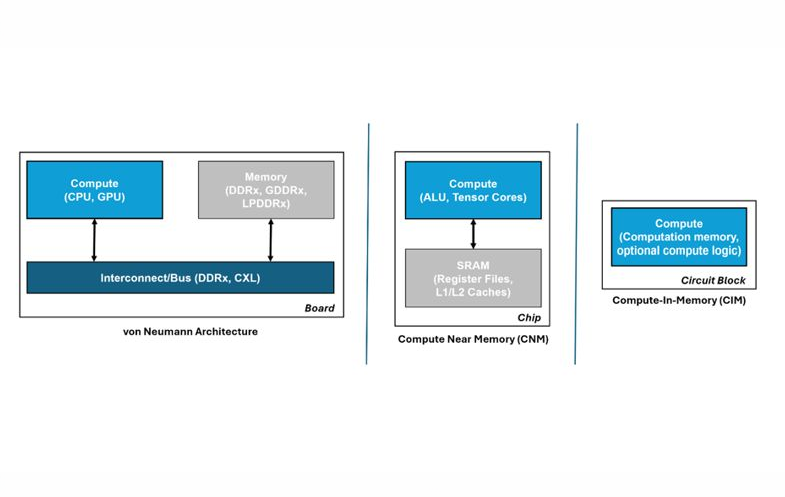
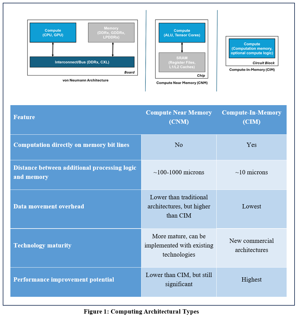
CIM differs from traditional von Neumann architectures in that computation is performed in or near memory, reducing data movement. This is particularly important for data-centric applications such as AI/ML, where the cost of moving data can dominate total system power and latency.
Figure 1 is a side-by-side conceptual illustration of the three architecture types:
GSI Technology Associative Processing Unit CIM Architecture
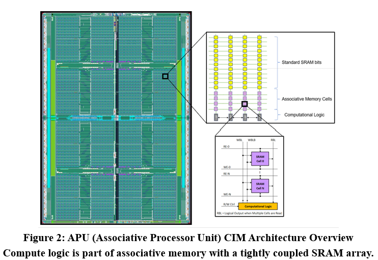
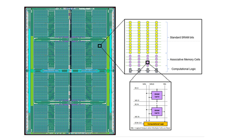
Figure 2 is an actual die photo of the GSI APU Gemini-I chip. The design leverages GSI's 28 years of experience in DRAM/SRAM. Unlike CPUs/GPUs, this architecture does not have disparate sections that require moving data around the chip.
APU bit processors are groups of specialized SRAM bits that are read simultaneously onto bit lines, enabling Boolean operations during the read process. There are 2 million bit-engines in the first-generation Gemini-I, capable of over 2 peta-operations per second at 500 MHz. Computing in-memory eliminates the memory transfer bottleneck that limits traditional architectures.
This architecture represents a departure from the traditional von Neumann model, where computation and storage are separate. In this CIM architecture, computation and storage occur in-place within the bit processor array.
APU Applications
The benefits of compute-in-memory extend across AI/ML, vector search, real-time analytics, image classification, and high-performance computing (HPC) applications including synthetic aperture radar (SAR), genomics, and cryptography.
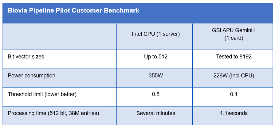
Gemini-I has been used in Biovia Pipeline Pilot for drug search using Tanimoto-based distance measures. [1]
GSI's Fast Vector Search (FVS) library and API support traditional vector search and SHA processing for password recovery.
Gemini-I has been used in high-performance computation for Synthetic Aperture Radar image generation on 1U mobile servers.
The University of Northern Arizona published work on cryptographic processing using this architecture. [2]
Cornell University published a circuit-based exposé on bit-matching for DNA Read Mapping. [3]
These examples demonstrate the industrial relevance of APU technology for real-time processing and performance/watt/$ efficiency.
GSI's APU-CIM Architecture Advantages and Business Value
GSI's APU represents a paradigm shift, offering associative, massively parallel, true compute-in-memory capabilities.
High power efficiency and low power consumption:
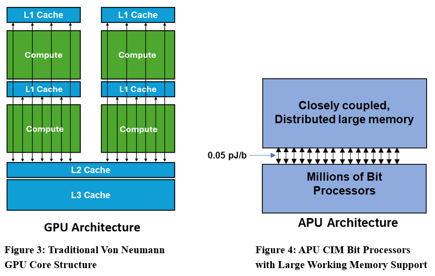
The architecture computes data in memory, achieving Boolean operations at single clock rates. Compared to traditional von Neumann GPUs, the APU architecture involves memory transfers of only 20 microns apart. This tremendously fast processing array can also be loaded from register memory. As this memory is very large, larger than the in-place computation memory, and it is distributed and about 100 microns away from the processing memory, again we see about two to three orders of magnitude less movement of data resulting in faster processing and much lower power consumption. This data transfer on the first-generation APU amounts to about 0.05 pico-Joules per bit.
Flexibility
The APU architecture does not inflict a pre-defined framework on the programmer. Instead, any framework, including custom bit widths down to single bits, can be used natively in the device. Multiple different bit widths can then be devised using this methodology to allow even cycle-by-cycle dynamic precision to conserve compute and memory resources without sacrificing accuracy. This provides for futureproofing in the ability to create algorithms on bit widths that may not even be considered yet. An example of natively supporting new architectures is the ability to support the Microscaling Format (MX Format). This architecture can also handle Binary Neural Network (BNN) frameworks now.
Sustainable Application Performance
The combination of millions of bit processors in the APU array and the large, closely coupled distributed memory means that the architecture is capable of eliminating application memory bottlenecks for models that can be housed in its array. This leads to 100% core utilization, highest throughput, and lowest power consumption. The second-generation Gemini-II incorporates 96MB of register memory allowing single devices to address larger models at the edge, or building out datacenter systems that can address very large models at full core utilization.
Scalability
Because compute-in-memory devices are memories in one aspect, systems utilizing these components can scale as you would add memory to a system—by merely adding more components and without the need for complex connectivity. Using this methodology, it becomes quite normal to have a single low-cost server system with 8 or 16 cards in place. Massive scaling now becomes possible with commodity 10gE server interconnects.
These benefits compound to allow users to build systems from the edge to datacenter deployments with the best TCO (performance/W/$).
Source: GSI Technology, Inc.
Comparisons
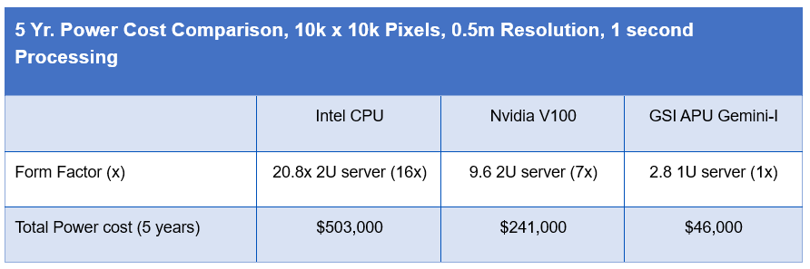
High Performance Compute example: Synthetic Aperture Radar Processing
Distinguished by: Varying "random" variable precision, parallel processing, one-to-all sensor data input to processors
Custom Search Application: Small Molecule Drug Discovery
Distinguished by: Desired low threshold comparison, large vector lengths: tested to 8000-bit widths
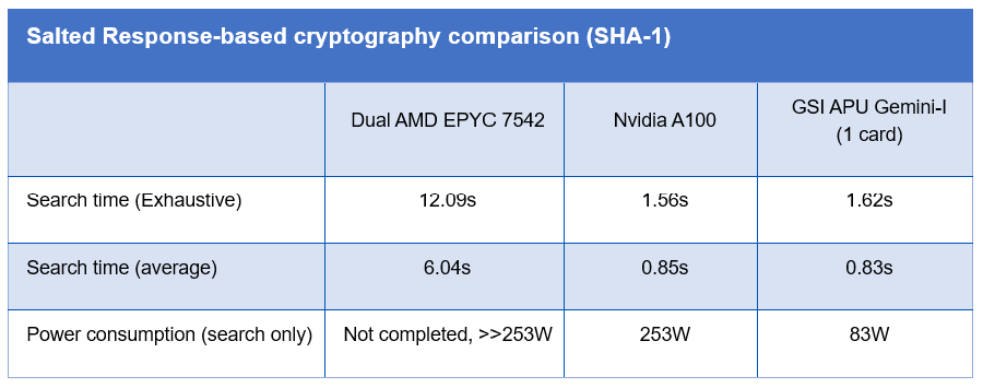
High Performance Compute: Salted Response-based Cryptography Comparison (SHA-1)
Distinguished by: Cryptography processing
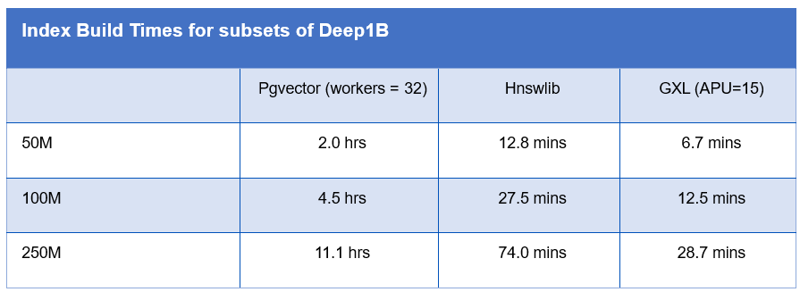
HNSW Index Build Acceleration
Distinguished by: Parallelism and hardware graph build acceleration
Conclusion
GSI's in-memory computing represents a significant shift in computing paradigm with proven SRAM technology that is ready for high volume deployment. As the cost of traditional compute and memory in terms of energy, cooling, and diminishing returns on scale continues to increase, in-memory computing has been proven to be able to more efficiently take on traditional von Neumann processing workloads and is becoming an increasingly vital component of modern IT infrastructure, enabling applications and actions that were previously economically unattainable.
We've covered several application types that this technology has shown differentiable performance—sometimes orders of magnitude—better than traditional compute. Of particular importance is this technology to three types of processing: Inference workloads that are accelerated with softmax can be handled natively with Tanimoto classification; high performance computations based on or that can be efficiently transformed into binary representative processing; and processing that can be categorized by high repetitive loops, particularly with one or both of the previous differentiators.
Source: GSI Technology, Inc.
For more information, please contact info@upmic.io
[1] https://gsitechnology.com/wp-content/uploads/sites/default/files/files/GSIT-Weizmann-Case-Study.pdf
[2] https://jan.ucc.nau.edu/mg2745/publications/Lee_DUAC_ICPPW2023.pdf
[3] https://gsitechnology.com/wp-content/uploads/sites/default/files/files/Accelerating-Seed-Location-Filtering-in-DNA-Read-Mapping-Using-Commercial-Compute-in-SRAM-Architecture.pdf